

If you’ve ever wanted to create your own custom PCB, look no further. In this article, we’ll guide you through the intricate process of designing a personalized circuit board.
From understanding the basics to implementing best practices, we’ll provide you with all the information you need to bring your ideas to life.
So grab a pen and paper, because it’s time to dive into the world of PCB design and make your mark in the electronic realm.
Understanding the Basics of PCB Design
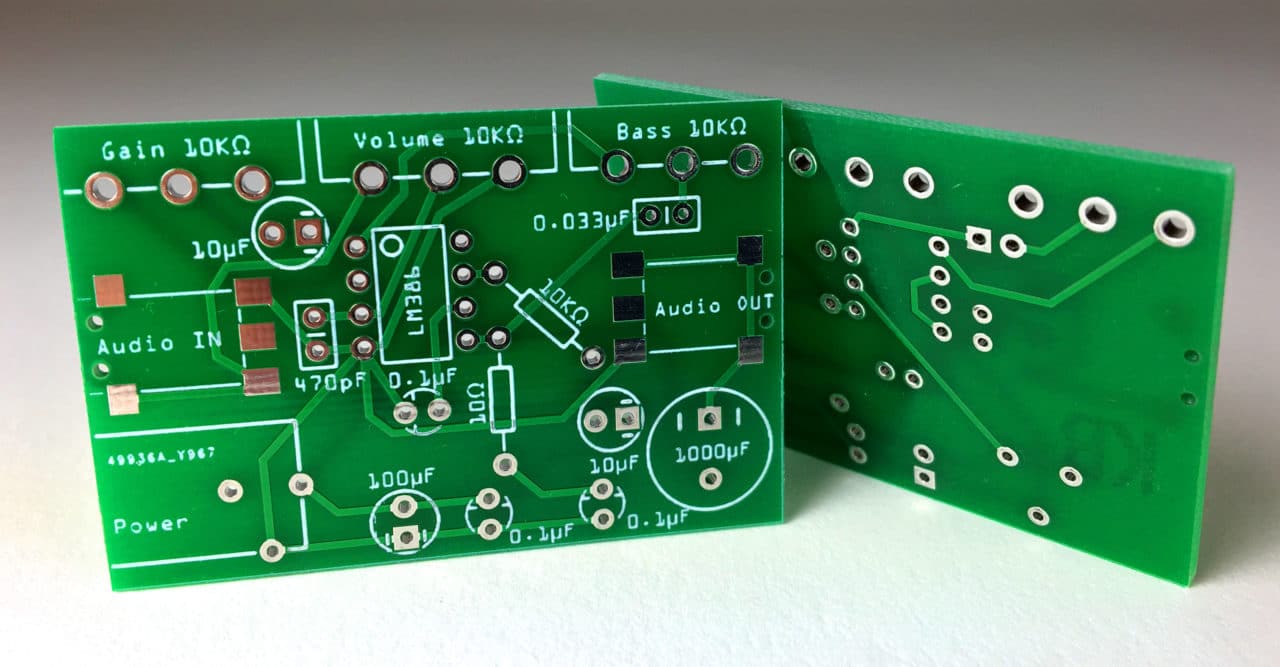
Understanding the basics of PCB design is essential for creating a custom circuit board. When designing a PCB, you need to consider various factors such as component placement, signal routing, and power distribution.
Proper component placement ensures optimal functionality and efficient use of space on the board. Signal routing involves connecting different components in a way that minimizes noise interference and maximizes signal integrity. It is important to carefully plan the path of each trace to avoid cross-talk and ensure proper grounding.
Additionally, power distribution must be carefully managed to ensure stable voltage levels throughout the circuit. By understanding these basic principles of PCB design, you can create a custom circuit board that meets your specific requirements while maintaining reliability and performance. Just like an experienced custom pcb designer.
Planning and Layout Considerations for Custom PCBs
To efficiently plan and lay out your custom circuit board, consider the specific requirements and constraints of your project. Here are four important considerations to keep in mind:
1. Component Placement: Arrange the components strategically on your PCB to optimize signal flow and minimize interference. Proper placement ensures efficient routing and minimizes crosstalk.
2. Trace Routing: Plan the paths for electrical traces carefully to avoid signal degradation or noise interference. Use a grid system to maintain consistency and symmetry in trace widths and spacing.
3. Power Distribution: Design an effective power distribution network that ensures stable voltage levels across the entire board. Consider factors like current capacity, decoupling capacitors, and ground plane placement.
4. Mechanical Constraints: Take into account any physical limitations or environmental factors that may impact your PCB design, such as size constraints, mounting requirements, thermal management, and EMI shielding.
Implementing Best Practices for Designing a Custom PCB
When implementing best practices for your custom circuit board, consider the specific requirements and constraints of your project to ensure optimal performance and reliability.
Begin by thoroughly understanding the functionality and purpose of your PCB. Identify the key components, their interconnections, and power requirements.
Take into account factors such as temperature, humidity, and electromagnetic interference that might affect your design.
Use industry-standard software tools to create a schematic diagram that accurately represents the circuitry and connections.
Pay attention to signal integrity by properly routing high-speed signals while minimizing noise coupling between different circuit sections.
Ensure proper grounding techniques are employed to minimize electrical noise interference.
Perform thorough testing and verification at each stage of development to identify any potential issues early on.
Conclusion
To conclude, designing a custom PCB requires a solid understanding of the basics and careful planning. By following best practices and considering layout considerations, you can create a high-quality PCB that meets your specific requirements.
While some may argue that designing a custom PCB is time-consuming and complex, it is important to remember that the benefits far outweigh the challenges. With attention to detail and technical expertise, you can successfully design a custom PCB that will enhance your electronic projects with precision and efficiency. Additionally, utilizing tools like a siglent oscilloscope during the testing phase can provide valuable insights into signal integrity and performance, ensuring the overall success of your electronic design.