
A Brief History of PCBs
Printed circuit boards, or PCBs, have been around for over 100 years. The first patented PCB was created in 1903 by a German inventor named Albert Hanson. However, it wasn’t until the 1940s that PCBs began to be used more widely in technology.
During World War II, the US military started using them in radios and other communication equipment. By the 1950s, they had become a standard component in electronic devices.
The Importance of PCBs in Modern Technology
PCBs are an essential part of modern technology as they allow for the creation of complex electronic circuits that are compact and efficient. They allow for the easy integration of microprocessors, memory modules and other electronic components into a single unit. This means that today’s computers, smartphones and other devices can operate quickly and efficiently with minimal space usage.
PCBs are also incredibly versatile; they can be designed to fit almost any application or requirement. From simple single-layer boards to complex multi-layered ones with intricate routing paths, there is a PCB solution suitable for every need.
An Overview of PCB Manufacturing Process
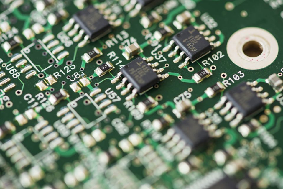
The manufacturing process for printed circuit boards is complex and requires specialized tools and equipment. It typically involves a printed circuit board company doing four main steps: pre-production stage, copper deposition stage, drilling stage and plating stage.
During the pre-production stage, designers use CAD software to create schematics which are then converted into Gerber files. These files contain all the information needed for the manufacturing process.
The next step is copper deposition where copper is applied to a substrate material such as FR4 or polyimide using a process called electroplating. This creates conductive pathways that will later form electrical connections between components on the board.
In drilling stage holes are made through the substrate for vias and other through-hole components. In the plating stage, a thin layer of metal is deposited over the circuit board to protect it from oxidation and corrosion.
Printed circuit boards are a crucial component of modern technology. They enable the creation of compact and efficient electronic devices by allowing for easy integration of complex circuits into a single unit.
The manufacturing process is complex but allows for versatility in design and application. With constant advancements in technology, the significance of PCBs will continue to grow exponentially.
Designing a PCB
Designing a printed circuit board (PCB) can seem like a daunting task, but with the right tools and knowledge it doesn’t have to be. The first step in designing a PCB is choosing the right CAD software. There are many options available, both paid and free, each with their own strengths and weaknesses.
Some popular choices include Eagle PCB, Altium Designer, and KiCad. Once you have chosen your CAD software, it’s time to start designing the schematics and layouts for your PCB.
This involves creating a visual representation of your circuit using symbols for components such as resistors, capacitors, and transistors. You will also need to determine the layout of your components on the board itself.
When designing a PCB, there are several important design considerations that must be taken into account. Trace width/spacing is one such consideration – this refers to the width of the copper traces that connect different components on the board.
It’s important to choose an appropriate trace width based on factors such as current requirements and signal frequency. Via placement is another crucial consideration when designing a PCB.
Vias are small holes drilled through the board that allow signals to pass from one layer to another. Proper via placement can help reduce noise in high-frequency circuits and ensure reliable connections between layers.